Low-frequency electronic noise is a problem in many devices and circuits but researchers are still unsure as to whether this noise is generated on the surface of electrical conductors or inside the bulk of a device. A team led by Alexander Balandin at the University of California Riverside (UCR) has now shed more light on this almost century-old question thanks to noise measurements on atomic graphene multilayers. The findings will be invaluable for making electronic devices smaller than a few nanometres in size and for graphene-based analogue circuits, communication networks and sensors.
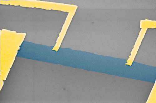
The device
“Unlike the thickness of metal or semiconductor films, the thickness of graphene multilayers can be continuously and uniformly varied all the way down to a single atomic layer – which can be thought of just a surface with no bulk,” explained Balandin. “Multilayer graphene films, produced by mechanical exfoliation, have thus allowed us to study where low-frequency, or 1/f, noise actually comes from for the first time – the surface of a material or the bulk.”
Thanks to noise measurements on moderately doped graphene samples made up of between one to 15 atomic layers, the researchers found that 1/f noise originates on the surface for samples that contain less than seven layers. However, the noise originates inside the bulk of the sample when its thickness exceeds seven layers. This is an unexpected discovery, says Balandin, because seven atomic layers represent a film that is around just 2.5 nm thick. “Our results have revealed a scaling law for 1/f noise that will be important for miniaturizing nanoscale devices in general, even though our measurements were only made on graphene multilayers.”

Alexander Balandin
Decreasing device size = more noise
Low-frequency, or 1/f, noise was first discovered in vacuum tubes almost 100 years ago and appears to occur in most electronics and communications devices as fluctuations in the electrical current. 1/f noise levels strongly increase as device size decreases. This is a real problem because the feature sizes of conventional devices, such as silicon complementary metal-oxide-semiconductor (CMOS) transistors, are becoming ever smaller, so that more of these devices can be packed onto an individual chip. Increases in 1/f noise are not only detrimental for transistors and interconnects in digital circuits but also for high-frequency circuits such as mixers and oscillators, where 1/f noise up-converts into phase noise and deteriorates the signal-to-noise ratio in operational amplifiers and analogue-digital converters.
Modern transistors typically have a thickness of around a nanometre, so it is important to understand when 1/f noise becomes a purely surface effect. Although the exact thickness may vary from material to material, the length scale at which a transistor channel or barrier layer starts to behave like a surface (for where noise is concerned) will be important for designing next generation electronics.
Balandin and colleagues findings will also be important for making graphene-based analogue circuits, communication networks and sensors, because all these applications require acceptably low levels of 1/f noise.
The team, which includes researchers from the Rensselaer Polytechnic Institute (RPI) and the Ioffe Physical-Technical Institute of The Russian Academy of Sciences, initially planned to investigate how 1/f noise levels scale with the thickness of graphene multilayer films. “We then realized that our results could provide an insight into the origins of 1/f noise itself and answer the almost century-old surface versus volume question,” Balandin told nanotechweb.org.
“We would now very much like to decipher the exact physical mechanisms behind the 1/f noise because there is still no universally accepted theory,” he added.
The work is published in Applied Physics Letters.